Search & find:
Media, press releases, events for your editorial coverage

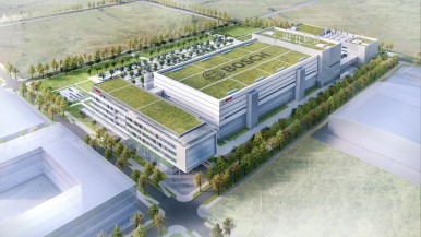
300 milimeters wafer fab in Dresden

21.08.2023

Factsheet

Connected mobility

300 milimeters wafer fab in Dresden

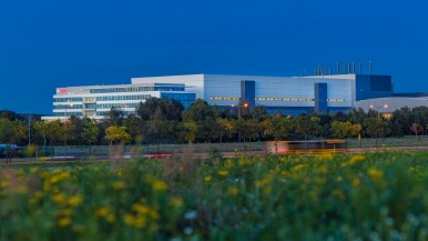
Total investment approx. 1 billion euros Site approx. 100,000 m2 Total floor space approx. 72,000 m2 of production area and office space Clean-room area Currently approx. 10,000 m², addition of some 3,000 m² Associates roughly 480 in August 2023 Qualified professionals needed Experts from the semiconductor industry, such as process, production or maintenance engineers, mathematicians, software engineers as well as professionals and graduates with degrees in physics, chemistry, or microsystems technology Manufactoring technology Highly automated wafer production (300mm silicon substrate wafers with structures up to 65nm in width) Manufactured products Application-specific integrated circuits (ASICs) and power semiconductors MEMS manufactoring on 300mm wafers (SOP in 2026) Fields of application for semiconductors Mainly automotive electronics and industrial applications Connected manufactoring At the wafer fab in Dresden, production data is generated at a rate of 250 MB/second, which corresponds to the data volume of 400 HD videos running simultaneously. Funding Construction of the new wafer fab in Dresden received funding as part of IPCEI 1 Microeletronics (Important Project of Common European Interest) from the German federal government – more specifically, the Federal Ministgry for Economic Affairs and Climate Action (BMWK). Over the next years, Bosch plans to invest some three billion euros in Dresden and Reutlingen, both as part of its own investment plan and under the auspices of the European IPCEI ME (“Important Project of Common European Interest on Microelectronics”) funding program.

Reutlingen wafer fab

28.10.2021

Factsheet

Connected mobility

Reutlingen wafer fab

Areas of operation Manufacturing for semiconductors (Frontend) Test center for semiconductors (Backend) Associates about 4,000 Cleanroom surface area 35,000 m², till end of 2025: 44,000 m² Production facilities 150-millimeter technology since 1995 200-millimeter technology since 2010 Pre- and final measurement for 150- and 200-millimeter wafers Manufactured products Application-specific integrated circuits (ASICs), low-voltage/high-voltage power semiconductors, microelectromechanical systems (MEMS) Manufacturing technology 150- and 200-millimeter silicon substrates with structural widths (nodes) of up to 180 nanometer 150-millimeter silicon carbide substrates with structural widths (nodes) of up to 400 nanometer Fields of application for semiconductors Power units for electromobility, e-bikes, power tools and further Bosch products Automotive electronics: airbag and driver assistance systems, Electronic Stability Control ESC, electronic control units for electric motors and IC engines as well as for transmissions, parking assistants and night vision enhancement systems Consumer electronics: games consoles, hearables, laptops, smartphones, wearables Investments and extension course of action Rising demand Consistent development of the manufacturing capacity to meet the growing demand of semiconductors chips (ASICs, MEMS and power semiconductors). From 2021 to 2023 With 150 million euros in two steps from 2021 to 2023 will gain about 4,000m² of new cleanroom surface area that will be realized in existing buildings. In addition, 150 new jobs in the fields of semiconductor development will be raised. Till end of 2025 State-of-the-art manufacturing: more than 250 million euros will be invested for a new element, the total amount of the cleanroom surface area will raise up to 44,000 m².

Semiconductor production at Bosch

28.05.2021

Factsheet

Connected mobility

Semiconductor production at Bosch

Current portfolio Bosch manufactures and sells electronic components for vehicles and for consumer electronics. These include application-specific integrated circuits (ASICs) , power semiconductors and microelectro-mechanical systems (MEMS) such as acceleration, pressure, yaw-rate, magnetic field, mass-flow and environ-mental sensors. Manufacturing sites Reutlingen (150-mm and 200-mm technology) Dresden (300-mm technology) Patents Bosch holds more than 1,000 patents and patent applications for MEMS technology as well as more than 500 in the field of semiconductor technology. Market The requirements after semiconductor chips (ASICs, power semiconductors and MEMS) will further increase. The reason is about a rise of the proportion of semiconductors in electronic devices and car applications, e.g. connected and automated driving or the electro mobility. Microelectronics can be seen as technological key sector. Expertise in innovation and technology Invented for life For more than 60 years Bosch has been developing and manufacturing microelectronic components and systems. In 1958 the first semiconductor product a “Variode” was produced in Stuttgart-Feuerbach. Semi-conductors (integrated circuits) have been manufactured at the wafer fab in Reutlingen since 1970. Know-How in semiconductor’s business Microelectronics: Bosch is making key business Technologies accessible and is inventing innovative production measures. The company developed the microfabrication technique called “Bosch Prozess” in 1994 where new semiconductors can be manufactured. Sensor technology Since 1995 Bosch has been producing more than 15 billion MEMS and is now the world market leader in this field. “Deutscher Zukunftspreis 2008“ Award winning invention of a new procedure for the surface micromechanics. First AIot-plant in Dresden In 2021 Bosch opened one of the most modern wafer fab in the world: a highly automated and intelligent plant, with fully connected machines and embedded processes combined with artificial intelligence methods. New innovation in series At the end of 2021: start of production of Silicon carbide (SiC) semiconductors which are used in the power electronics of electric cars reaching more range and faster charging stops. Vertical synergies Bosch is one of the leading suppliers in the automotive industry with an own sector for semiconductors. Investments Capital expenditure In its wafer fabs in Reutlingen and Dresden alone, Bosch has invested more than 2.5 billion euros since 200-millimeter technology was introduced in 2010. On top of this, billions of euros have been invested in developing microelectronics. 2021 The wafer fab Dresden is the biggest single Investment of the company’s history with about one billion euros of investment. Till 2023 in Reutlingen: more than 150 million euros will be invested for new cleanroom surface areas in existing buildings and 150 new jobs in the fields of semiconductor development will be raised. 2022 More cleanroom surface areas for meeting the demand of chips: more than 400 million euros for the expansion in Dresden, Reutlingen, Penang. 2023 Expansion of the existing cleanroom surface area in Dresden for more than 250 million euros. Till end of 2025 State-of-the-art manufacturing: more than 250 million euros will be invested for a new element, the total amount of the cleanroom surface area will raise up to 44,000 m².

Semiconductor terminology

25.05.2021

Factsheet

Connected mobility

Semiconductor terminology

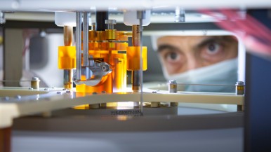
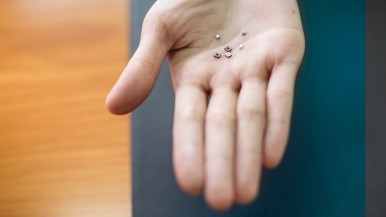
Semiconductors – one way, then another Semiconductors are chemical substances that have the properties both of electrical conductors and of non-conductors – hence semiconductors. As microchips, they are built into practically every kind of electrical system. They are a key technology of the connected world. Silicon – the raw material of the connected world Silicon (Si) is the stuff of high-tech dreams. In the natural world, it is as common as sand on the beach – in fact, sand is mainly made up of silicon dioxide. To get the ultra-pure monocrystalline silicon needed for chip production, oxygen is extracted from the sand in a complex process. One metric ton of sand is enough to make roughly 3,000 wafers measuring 300 millimeters in diameter. Wafers – the semiconductor world in disc form In the world of semiconductors, the term “wafer” means a circular disc made of a material such as silicon. In what is known as a drawing process, a round monocrystal – the ingot – is created from extremely hot liquid silicon. The ingot may be 300 millimeters in diameter and more than one meter long. This cylinder is then sawed into discs – the raw wafers. These discs are thinner than a millimeter. In a manufacturing process lasting up to several month, these discs are turned into semiconductor chips. Semiconductor chips – and what they have to do with skyscrapers A microchip comprises many superimposed layers, like the stories of a skyscraper. Roughly 30 layers are stacked on top of each other in a microchip. Each of these has a particular function, such as conducting electricity or forming resistors. To create these layers, the wafer has to go through hundreds of process steps. In these steps, additional thin layers are deposited onto the wafer and structured. First, individual layers are deposited on the raw wafer, coated with photoresist, then exposed through a photomask. Only the exposed photoresist hardens, while the coating that has remained soft is removed by an etching solution. The surfaces that have been stripped in this way are now subject to physical processes, as a result of which the material there takes on the required electrical properties. Following that, any remaining photoresist is removed by cleaning. A new layer is now deposited on the wafer layer that has been treated in this way, and the process starts over – with a photomask for the next layer and the associated process. The more layers that are created, the more complex and powerful the chip will be. In this way, active and passive components are created on the wafer. Metal conductor tracks connect them with a circuit. It may take several months for a wafer to pass through all these process stages. All the circuits that have been created in this way are then checked for functionality while still on the wafer. The wafer is then sent to manufacturing partners, who break it up into individual chips and package them in their typical plastic housing. Following a further function test, the microchips are ready to be used in many electronic parts, components, and systems. MEMS – seeing, feeling, smelling Rectangular or square, smaller than a pinhead, and between one and four millimeters tall – the tiny MEMS sensors are hugely versatile all-around talents in the connected world. MEMS stands for microelectromechanical systems. They act effectively as sensory organs in a wide range of different applications in vehicles and supply the control units with important information, such as whether the car is spinning on a slippery road surface. Nowadays it is also impossible to imagine consumer and entertainment electronics without MEMS sensors. For example, they transform a simple cellphone into a smartphone that takes sharp photos with no shaking or jittering. MEMS sensors consist primarily of a MEMS element and an ASIC on a tiny circuit board. The whole object is covered by a protective casing. ASICs – chips with built-in “intelligence” If MEMS sensors are the sensory organs of the connected world, then application specific integrated circuits (ASICs) are the brains. They process the information from the MEMS sensors and trigger further actions. For example, they deploy a vehicle’s airbags at exactly the right time. Although the silicon chips measure just a few square millimeters, they contain complex circuits, sometimes featuring several millions of individual electronic functions. Power semiconductors – brimming with strength These special semiconductor components look after the controlling and switching of high electrical currents and voltages. To manage this, they are equipped with special switching and conducting properties, as the high currents and voltages would destroy ordinary semiconductor components. In electric and hybrid vehicles, for example, they control the energy flow in the power electronics between the battery and the e-motor and ensure that the electricity is used as efficiently as possible. Cleanrooms – not just clean, but squeaky clean Semiconductors are made up of extremely fine structures roughly 50 times thinner than a human hair. In the manufacturing rooms for semiconductor production, therefore, it must be ensured that there is absolutely no dust or other contaminating particles present in the ambient air. Even the tiniest of particles can destroy semiconductor components. Therefore, the air is kept clean using special extraction and filtering technology. There are various cleanroom classes. Sensitive chip manufacturing requires the purest: class 1. For work clothing, this means: coverall, gloves, hood, and face mask. And make-up, lipstick, and eyeliner are a no-go. Yellow light – without the sun The cleanroom is illuminated with a special yellow light that contains no ultraviolet radiation. This prevents the photoresist-coated wafers from being inadvertently exposed.

300 mm wafer fab in Dresden

30.09.2019

Factsheet

Connected mobility

300 mm wafer fab in Dresden

General information Total investment approx. 1 billion euros Site approx. 100,000 m2 (about 14 soccer fields) Total floor space approx. 72,000 m² of production area and office space Construction timeline Groundbreaking in spring 2018, installation of machinery mid-/end 2019, pilot production to start at end of 2021 Associates in the completed plant Up to 700 Qualified professionals needed Experts from the semiconductor industry, such as process, production, and maintenance engineers, mathematicians, software engineers, as well as professionals with degrees in physics, chemistry, and microsystems technologies Manufacturing technology Highly automated wafer production (300 mm silicon substrate wafers with structures up to 65 nm in width – 1 nm equals one millionth of a millimeter) Connected manufacturing Every second, the machines will transmit one gigabit of production data. The volume of data produced is equivalent to more than 42 million written sheets of paper, weighing 22 metric tons.Details on the building Total building volume 600,000 m³ Concrete approx. 66,500 m³ (about 8,300 concrete mixer trucks) Steel approx. 16,400 metric tons (about 30 A380 passenger jets) Earth moved/excavated approx. 90,000 m³ (some 7,500 truckloads) Bored piles for the foundation approx. 860 Floor slabs 100 cm thick Length of piping and ductwork approx. 80 km Length of electrical cabling approx. 380 km (from Dresden to Berlin and back)Internet For job seekers www.bosch-career.de/jobs Site for the Dresden location https://www.bosch.de/en/our-company/bosch-in-germany/dresden/ Bosch semiconductors http://www.bosch-semiconductors.com/

16.04.2019

Factsheet

Business/economy

Bosch Mobility Solutions in China’s automotive market

Bosch’s Mobility Solutions business sector performed well in a difficult market environment in China in 2018. Sales rose to 10.5 billion euros, accounting for a 1 percent increase year on year1 and roughly 22 percent of Bosch Mobility Solutions’ global sales. As a result, China is the most important foreign market for Bosch’s Mobility Solutions business sector. Bosch maintains 38 manufacturing sites in China, with 23 plants making products for Mobility Solutions. The business sector’s largest manufacturing site is in Suzhou, where 9,800 associates produce ABS and ESP systems, as well as display instruments, to name just a few examples. Of the 27 Bosch research centers in China, 18 are working on new mobility solutions. In China, Bosch employs some 60,000 associates in total – its largest workforce outside Germany. Roughly 34,500 associates work for Bosch Mobility Solutions in China, or 15 percent of all the business sector’s associates. In addition, more than 5,600 researchers and engineers in China are working on new mobility solutions. In late March 2019, Bosch opened a new plant for the iBooster electromechanical brake booster in Nanjing. The company invested 100 million euros in the plant, which measures some 20,000 square meters. Mass production of the 48-volt battery began in Wuxi in 2018. Production of the e-axle is slated to start in Taicang this year. Bosch continues to expect good opportunities and tremendous potential for its Mobility Solutions business sector in China in the medium to long term. The Chinese automotive market is far from being saturated, with roughly 170 vehicles for every 1,000 inhabitants. In Germany, that figure stands at approximately 690 vehicles per 1,000 inhabitants. Bosch is celebrating its 110th anniversary in China in 2019. Twenty-five years ago, Bosch also founded its first joint ventures with Chinese partners, making it a manufacturing company in China. Facts about the automotive market in China Since 2009, the Chinese vehicle market has been the largest in the world – well ahead of Europe and the U.S. In 2018, 23.7 million cars were sold in China, along with 4.4 million light and heavy commercial vehicles (source: CAAM). In 2018, 1.26 million new energy vehicles (NEVs) – battery-powered electric vehicles, plug-in hybrids, and fuel-cell cars – were sold in China, representing an increase of more than 50 percent year on year and 5.3 percent of the overall market (source: CAAM). Of the 20 largest brands in China, domestic manufacturers accounted for 39 percent of all cars sold in 2018. European manufacturers accounted for 31 percent, with 14 percent going to Japanese brands, 11 percent to U.S. brands, and 5 percent to Korean makers. At 477,000 units, the best-selling car in China in 2018 was the family van Wuling Hongguang made by SGMW – a joint venture between SAIC Motor, General Motors, and Liuzhou Wuling Motors. Most people in China spend between 50,000 and 150,000 Chinese yuan (6,500 to 20,000 euros) on a new car. In Germany, car buyers invest an average of over 30,000 euros in a new vehicle. At roughly 50 percent of the total market, SUVs and vans were the most popular vehicle segment in China in 2018, followed in second place by mid-sized vehicles, which accounted for a share of approximately 29 percent (source: CAAM). Quotes by Bosch management board member Dr. Stefan Hartung: “Today, China is the center of the global automotive industry. The Chinese automotive market is evolving into a lead market for modern mobility in which Bosch plans to play an important role.” “The brakes will stay on in the Chinese automotive market this year. After two decades of constant growth, the market is taking time out in 2019. Still, the potential and the opportunities for Bosch in China remain tremendous in the medium to long term.” “The future of mobility needs inventors, not slowpokes. China is producing more and more inventors, and Bosch is in high demand as a strong partner.” “China’s automakers have gone from baby steps to seven-league strides in a remarkably short time. Soon they will no longer be mere onlookers in the global market.” “Bosch is at home in Germany. It also has deep roots in China – having been there for 110 years.”


25.06.2018

Factsheet

Business/economy

Bosch in Brazil

About Hermann Scholl: Hermann Scholl has been the honorary chairman of the Bosch Group since mid-2012. Prior to that, he was chairman of the board of management of Robert Bosch GmbH until 2003 and, until 2012, chairman of the supervisory board of Robert Bosch GmbH and managing partner of Robert Bosch Industrietreuhand KG since mid-1995. Further informationQuotes: “ It has been some 25 years since I worked very closely with Bosch Brazil in my role as chairman of the board of management at Bosch. I am delighted that the German-Brazilian Chamber of Commerce still takes such a positive view of that time. This award is an honor for me. ” “ Bosch can look back on a long and successful history in Brazil. ” “ Brazil is a wonderful country with many impressive highlights. I remember the people as very endearing, open, and pragmatic. ” Bosch looks back on a long and successful history in Brazil Tradition: Bosch opened its first branch office in Brazil in 1910. The local subsidiary Robert Bosch Ltda. was established in 1954. The headquarters of Bosch Brazil, which remain responsible for the entire Latin America region to this day, were built just a few years later in Campinas, near São Paolo. Bosch has thus been active in Brazil for more than 100 years. All four business sectors operate there today. Local presence: In Brazil, the company focuses on localization. In Campinas, Bosch manufactures mobility solutions such as vehicle retrofitting components, powertrain systems, driver assistance systems, and power tools. The plant in Curitiba produces diesel injection systems. Aratu makes spark plugs, and Pomerode is home to a plant for hydraulic systems. Since 2010, the Bosch service center in Joinville has been providing service solutions for South America. Sales: A successful business year in 2017: sales rose to 4.9 billion reais (1.4 billion euros), with exports accounting for 28 percent in total. Bosch’s business in Brazil accounted for 80 percent of total sales in Latin America. The Mobility Solutions business sector in particular saw positive developments in 2017 due to growth in vehicle production in Brazil and Argentina. Investment: In 2017, Bosch invested some 53 million euros in Brazil. Headcount: Bosch employs some 8,300 associates in Brazil at 14 locations. Dual education model at Bosch in Brazil: In 1960, Bosch became one of the first companies to set up a dual education system in Campinas and Curitiba. Using this model, which is well-established in Germany, we train professionals such as mechatronics engineers according to German standards. To date, a total of over 1,400 young people have accordingly completed their occupational training. Bosch has also opened a center in Campinas that conveys and enhances knowledge throughout the spectrum of industrial occupations to facilitate efficient training. In addition, Bosch Brazil supports the promotion of talent and occupational training programs in the country. Local innovation: Strong localization is an important part of the Bosch strategy worldwide. The electronic control system for the flex-fuel engine is a good example of this. In 2003, Bosch developed a unique local solution for Brazil with this innovation, which allows drivers to choose flexibly between gasoline and ethanol at the pump. As a vehicle fuel, ethanol continues to have tremendous economic significance for Brazil. The flex-fuel engine is still used in most of the vehicles manufactured in Brazil. Smart solutions for Brazil: Demand for connected products is also growing in Latin America. In Brazil, Bosch is developing connected solutions for mining, logistics, and Industry 4.0. For the field of smart farming, Bosch offers a sensor system that reports animals’ weights to farmers and increases productivity on farms in Brazil. Corporate social responsibility: In Campinas, Bosch established the Centro Medico hospital in 1973. Originally set up to improve medical care for Bosch associates, the hospital was spun off into a foundation in 2004, ultimately opening it up to the general public. Instituto Bosch, which makes project funding of up to 3.5 million reais available every year, was also established in 2004. The school and vocational training projects it funds help to improve career opportunities for some 7,700 children and young people. The Primavera aid organization, established and financed by Bosch associates, operates worldwide and also receives donations from Brazilian associates. In Brazil, Primavera supports projects that are spearheaded by NGOs and schools, allowing it to reach an additional 2,000 children nationwide.

25.06.2018

Factsheet

Business/economy

Laying the foundation stone for 300 mm wafer fab in Dresden

General information Total investment approx. 1 billion euros Site approx. 100,000 m2 (about 14 soccer fields) Total floor space approx. 72,000 m² of production area and office space Construction timeline Groundbreaking in spring 2018 installation of machinery mid-/end 2019 pilot production to start at end of 2021 Associates in the completed plant Up to 700 Qualified professionals needed Experts from the semiconductor industry, such as process, production, and maintenance engineers, mathematicians, software engineers, as well as professionals with degrees in physics, chemistry, and microsystems technologies Manufacturing technologye Highly automated wafer production (300 mm silicon substrate wafers with structures up to 65 nm in width – 1 nm equals one millionth of a millimeter) Connected manufacturing Every second, the machines will transmit one gigabit of production data. The volume of data produced is equivalent to more than 42 million written sheets of paper, weighing 22 metric tons.Details on the building Total building volume 600 000 m³ Concrete approx. 66,500 m³ (about 8,300 concrete mixer trucks) Steel approx. 16,400 metric tons (about 30 A380 passenger jets) Earth moved/excavated approx. 90,000 m³ (some 7,500 truckloads) Bored piles for the foundation approx. 860 Floor slabs 100 cm thick Length of piping and ductwork approx. 80 km Length of electrical cabling approx. 380 km (from Dresden to Berlin and back)Internet For job seekers www.bosch-career.de/jobs Site for the Dresden location https://www.bosch.de/en/ourcompany/bosch-in-germany/dresden Bosch semiconductors www.bosch-semiconductors.com