Search & find:
Media, press releases, events for your editorial coverage

300 mm wafer fab in Dresden

30.09.2019

Factsheet

Connected mobility

300 mm wafer fab in Dresden

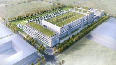
General information Total investment approx. 1 billion euros Site approx. 100,000 m2 (about 14 soccer fields) Total floor space approx. 72,000 m² of production area and office space Construction timeline Groundbreaking in spring 2018, installation of machinery mid-/end 2019, pilot production to start at end of 2021 Associates in the completed plant Up to 700 Qualified professionals needed Experts from the semiconductor industry, such as process, production, and maintenance engineers, mathematicians, software engineers, as well as professionals with degrees in physics, chemistry, and microsystems technologies Manufacturing technology Highly automated wafer production (300 mm silicon substrate wafers with structures up to 65 nm in width – 1 nm equals one millionth of a millimeter) Connected manufacturing Every second, the machines will transmit one gigabit of production data. The volume of data produced is equivalent to more than 42 million written sheets of paper, weighing 22 metric tons.Details on the building Total building volume 600,000 m³ Concrete approx. 66,500 m³ (about 8,300 concrete mixer trucks) Steel approx. 16,400 metric tons (about 30 A380 passenger jets) Earth moved/excavated approx. 90,000 m³ (some 7,500 truckloads) Bored piles for the foundation approx. 860 Floor slabs 100 cm thick Length of piping and ductwork approx. 80 km Length of electrical cabling approx. 380 km (from Dresden to Berlin and back)Internet For job seekers www.bosch-career.de/jobs Site for the Dresden location https://www.bosch.de/en/our-company/bosch-in-germany/dresden/ Bosch semiconductors http://www.bosch-semiconductors.com/


25.06.2018

Factsheet

Business/economy

Laying the foundation stone for 300 mm wafer fab in Dresden

General information Total investment approx. 1 billion euros Site approx. 100,000 m2 (about 14 soccer fields) Total floor space approx. 72,000 m² of production area and office space Construction timeline Groundbreaking in spring 2018 installation of machinery mid-/end 2019 pilot production to start at end of 2021 Associates in the completed plant Up to 700 Qualified professionals needed Experts from the semiconductor industry, such as process, production, and maintenance engineers, mathematicians, software engineers, as well as professionals with degrees in physics, chemistry, and microsystems technologies Manufacturing technologye Highly automated wafer production (300 mm silicon substrate wafers with structures up to 65 nm in width – 1 nm equals one millionth of a millimeter) Connected manufacturing Every second, the machines will transmit one gigabit of production data. The volume of data produced is equivalent to more than 42 million written sheets of paper, weighing 22 metric tons.Details on the building Total building volume 600 000 m³ Concrete approx. 66,500 m³ (about 8,300 concrete mixer trucks) Steel approx. 16,400 metric tons (about 30 A380 passenger jets) Earth moved/excavated approx. 90,000 m³ (some 7,500 truckloads) Bored piles for the foundation approx. 860 Floor slabs 100 cm thick Length of piping and ductwork approx. 80 km Length of electrical cabling approx. 380 km (from Dresden to Berlin and back)Internet For job seekers www.bosch-career.de/jobs Site for the Dresden location https://www.bosch.de/en/ourcompany/bosch-in-germany/dresden Bosch semiconductors www.bosch-semiconductors.com