Semiconductors – one way, then another
Semiconductors are chemical substances that have the properties both of electrical conductors and of non-conductors – hence semiconductors. As microchips, they are built into practically every kind of electrical system. They are a key technology of the connected world.
Silicon – the raw material of the connected world
Silicon (Si) is the stuff of high-tech dreams. In the natural world, it is as common as sand on the beach – in fact, sand is mainly made up of silicon dioxide. To get the ultra-pure monocrystalline silicon needed for chip production, oxygen is extracted from the sand in a complex process. One metric ton of sand is enough to make roughly 3,000 wafers measuring 300 millimeters in diameter.
Wafers – the semiconductor world in disc form
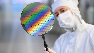
In the world of semiconductors, the term “wafer” means a circular disc made of a material such as silicon. In what is known as a drawing process, a round monocrystal – the ingot – is created from extremely hot liquid silicon. The ingot may be 300 millimeters in diameter and more than one meter long. This cylinder is then sawed into discs – the raw wafers. These discs are thinner than a millimeter. In a manufacturing process lasting up to several month, these discs are turned into semiconductor chips.
Semiconductor chips – and what they have to do with skyscrapers
A microchip comprises many superimposed layers, like the stories of a skyscraper. Roughly 30 layers are stacked on top of each other in a microchip. Each of these has a particular function, such as conducting electricity or forming resistors. To create these layers, the wafer has to go through hundreds of process steps. In these steps, additional thin layers are deposited onto the wafer and structured. First, individual layers are deposited on the raw wafer, coated with photoresist, then exposed through a photomask. Only the exposed photoresist hardens, while the coating that has remained soft is removed by an etching solution. The surfaces that have been stripped in this way are now subject to physical processes, as a result of which the material there takes on the required electrical properties. Following that, any remaining photoresist is removed by cleaning. A new layer is now deposited on the wafer layer that has been treated in this way, and the process starts over – with a photomask for the next layer and the associated process. The more layers that are created, the more complex and powerful the chip will be. In this way, active and passive components are created on the wafer. Metal conductor tracks connect them with a circuit. It may take several months for a wafer to pass through all these process stages. All the circuits that have been created in this way are then checked for functionality while still on the wafer. The wafer is then sent to manufacturing partners, who break it up into individual chips and package them in their typical plastic housing. Following a further function test, the microchips are ready to be used in many electronic parts, components, and systems.
MEMS – seeing, feeling, smelling
Rectangular or square, smaller than a pinhead, and between one and four millimeters tall – the tiny MEMS sensors are hugely versatile all-around talents in the connected world. MEMS stands for microelectromechanical systems. They act effectively as sensory organs in a wide range of different applications in vehicles and supply the control units with important information, such as whether the car is spinning on a slippery road surface. Nowadays it is also impossible to imagine consumer and entertainment electronics without MEMS sensors. For example, they transform a simple cellphone into a smartphone that takes sharp photos with no shaking or jittering. MEMS sensors consist primarily of a MEMS element and an ASIC on a tiny circuit board. The whole object is covered by a protective casing.
ASICs – chips with built-in “intelligence”
If MEMS sensors are the sensory organs of the connected world, then application specific integrated circuits (ASICs) are the brains. They process the information from the MEMS sensors and trigger further actions. For example, they deploy a vehicle’s airbags at exactly the right time. Although the silicon chips measure just a few square millimeters, they contain complex circuits, sometimes featuring several millions of individual electronic functions.
Power semiconductors – brimming with strength
These special semiconductor components look after the controlling and switching of high electrical currents and voltages. To manage this, they are equipped with special switching and conducting properties, as the high currents and voltages would destroy ordinary semiconductor components. In electric and hybrid vehicles, for example, they control the energy flow in the power electronics between the battery and the e-motor and ensure that the electricity is used as efficiently as possible.
Cleanrooms – not just clean, but squeaky clean
Semiconductors are made up of extremely fine structures roughly 50 times thinner than a human hair. In the manufacturing rooms for semiconductor production, therefore, it must be ensured that there is absolutely no dust or other contaminating particles present in the ambient air. Even the tiniest of particles can destroy semiconductor components. Therefore, the air is kept clean using special extraction and filtering technology. There are various cleanroom classes. Sensitive chip manufacturing requires the purest: class 1. For work clothing, this means: coverall, gloves, hood, and face mask. And make-up, lipstick, and eyeliner are a no-go.
Yellow light – without the sun
The cleanroom is illuminated with a special yellow light that contains no ultraviolet radiation. This prevents the photoresist-coated wafers from being inadvertently exposed.


